


Semiconductors
Full-spectrum semiconductor design services from RTL through post-silicon validation, delivering precision chip engineering at every layer.
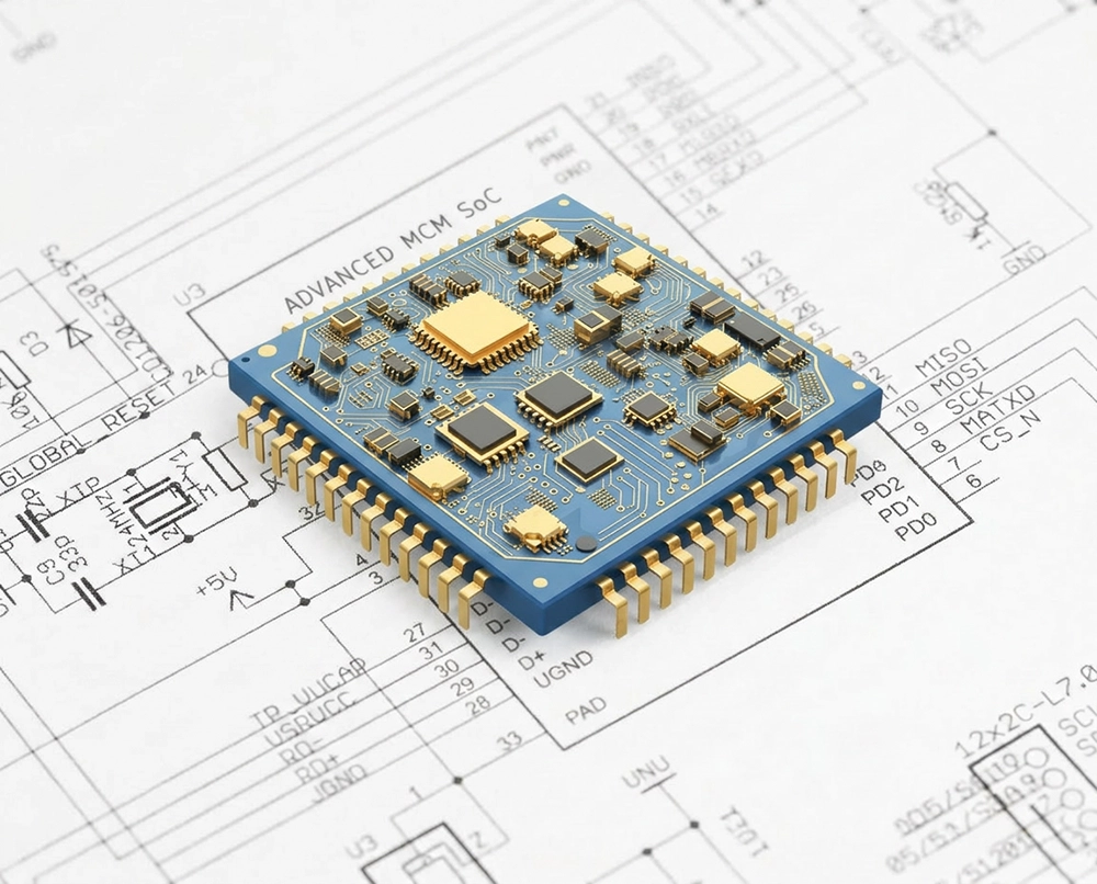
Semiconductor
RTL Design
The work spans custom IP, SoC subsystems, and protocol-driven blocks that must integrate cleanly with the rest of the chip. We keep the design intent clear, traceable, and easy to verify so the implementation flow stays predictable.That discipline helps teams move faster without accumulating hidden technical debt. The result is RTL that is easier to close, easier to reuse, and more resilient during verification and synthesis.
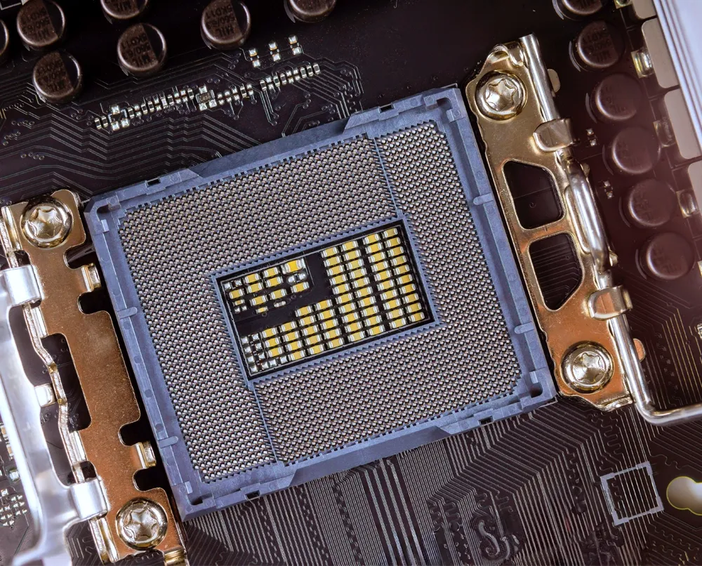
Physical Design
Our physical design work looks at the whole chip, not just isolated paths. We consider floorplan quality, clock structure, power distribution, and interconnect behavior so the final layout supports the original performance targets.That end-to-end view helps avoid costly surprises late in the schedule. It also improves the odds of first-pass success by aligning the design intent with real implementation constraints from the start.

FPGA Design
The focus is on practical hardware that can support high-speed interfaces, complex datapaths, and rapid iteration. We design with board-level realities in mind so the FPGA build remains reliable and useful in real development cycles.That makes FPGA work a bridge between architecture and production. It gives product teams a flexible way to validate ideas, reduce risk, and deliver value while the ASIC path continues in parallel.

Design Consulting
Consulting can cover everything from process-node selection to methodology setup and team ramp-up. We bring structured thinking to ambiguous problems and translate experience into concrete next steps for the program.That support is especially valuable when schedule pressure is high or the product scope is changing quickly. It gives teams a practical way to make progress with fewer blind spots and better alignment.

Design Verification
Our verification approach is built to expose corner-case failures before they become silicon problems. We combine structured methodology with strong debug discipline so issues are easier to isolate and fix.That reduces rework and improves first-pass quality. It also creates a clearer path from architecture to tape-out because every key requirement is traced through a verifiable flow.

DFT
The objective is not just to add test logic, but to make the chip manufacturable at scale. We pay attention to fault coverage, pattern volume, access strategy, and test time so production remains efficient.That preparation improves yield learning and helps teams uncover defects early. It also creates a smoother handoff into manufacturing because the silicon is built with testability in mind.
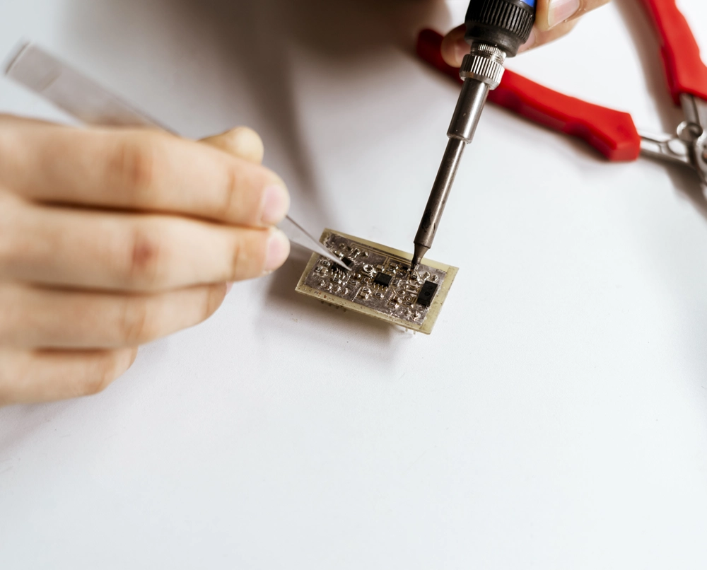
Post-Silicon Validation
The work includes bring-up, debugging, compliance checks, and data collection that reveal how the chip behaves in practice. We use those findings to pinpoint issues, verify fixes, and build confidence in the final product.Post-silicon validation closes the loop between design and reality. It turns assumptions into measured results and gives the team the evidence needed to release the product with confidence.
Driving Impact
Across Sectors
Healthcare
Finance
Retail
Manufacturing
Education